| 名称 |
MIRS1402 電源ボード詳細設計書 |
| 番号 |
MIRS1402-ELEC-0002 |
最終更新日:2014.12.19
| 版数 |
最終更新日 |
作成 |
承認 |
改訂記事 |
| A01 |
2014.12.19 |
廣瀬 |
青木先生 |
初版 |
目次
1.本ドキュメントについて
本ドキュメントは、MIRS1402の電源ボードについてのドキュメントである。
2.目的
回路面が汚くなっており、また基板をコンパクトにさせるため新規作成する。
3.回路設計
電源ボードの回路図を以下に示す。
circuit diagram
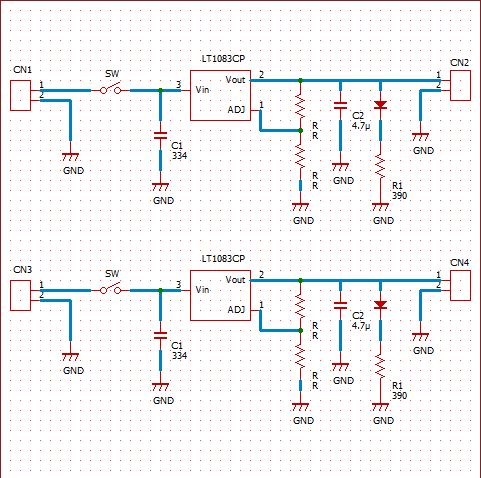
回路図より、Rとなっている場所は可変抵抗である。
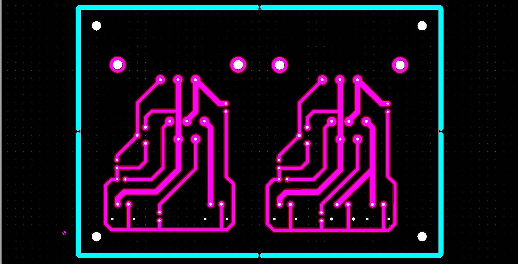
4.パターン図
電源ボードのパターン図を以下に示す。
circuit pattern generation
5.動作試験
1.MIRS1402 標準部品試験計画書にそって試験を行う。
6.試験結果
試験結果を
電源ボード結果に示す。
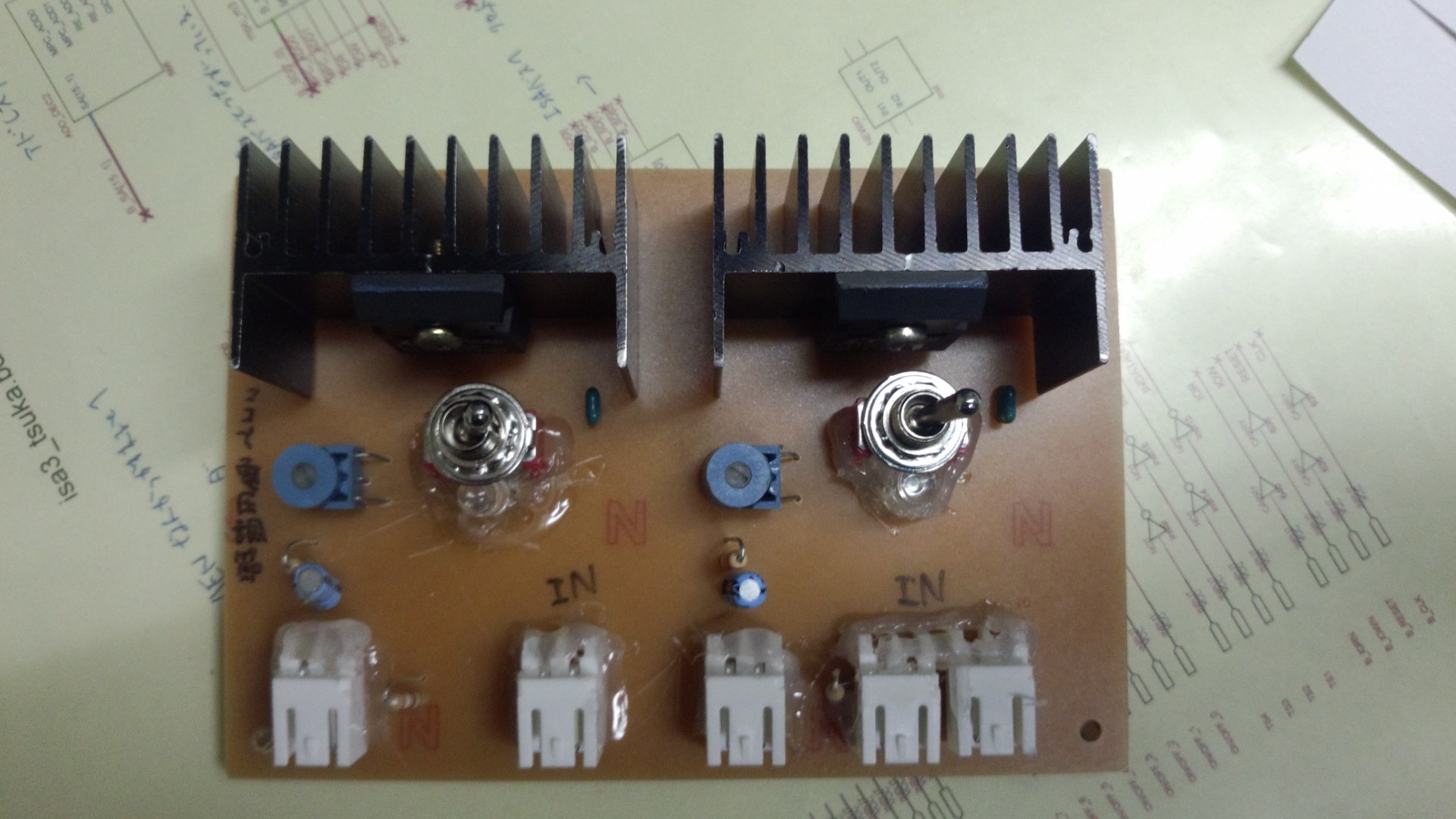
7.完成図
circuit pattern generation
沼津工業高等専門学校 電子制御工学科